
In the microelectronics and semiconductor industries, etching is a crucial step in the manufacturing process of chips, which determines the precision and performance of circuits. Etching processes are usually divided into two categories: wet etching and dry etching, each with its unique applicable scenarios and advantages.
Wet etching utilizes chemical reactions between liquid chemical reagents (etching solution) and the material being etched to selectively remove unwanted parts of the material surface. This process usually involves immersing the wafer to be processed in an etching solution, and precisely controlling the depth and contour of the etching by controlling parameters such as temperature, concentration, and time. Wet etching has the advantages of simple equipment and low cost, but it may not be as accurate and control complex patterns as dry etching.
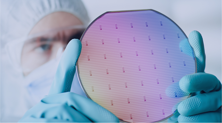
Dry etching does not rely on liquid media, but uses gases (such as fluoride, chlorine, etc.) or high-energy ion beams (such as plasma) to undergo physical or chemical reactions with the material surface, thereby removing the material. Dry etching includes various techniques such as reactive ion etching (RIE), deep reactive ion etching (DRIE), and plasma etching. These technologies can provide higher etching accuracy, better vertical sidewall contour control, and more complex pattern processing capabilities, making them widely popular in manufacturing high-precision and high-performance integrated circuits.
Etching, as a core technology in microelectronics manufacturing, its accuracy and reliability are crucial for the performance and yield of chips. With the advancement of technology, etching technology is also constantly developing to meet the growing demand for smaller and more integrated electronic products.